Band Structure of P-N Junction Semiconductor
Band Structure of P-N Junction Semiconductor


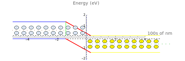
P-N Junctions are types of semiconductors with a unique band structure and are used in variety of applications from solar cells to LEDs to transistors. This Demonstration shows the electronic band structure, above, of a P-N junction as well as the physical junction, below, for a generic semiconductor. The left side, in blue, contains p-type dopant, which provides excess holes, brown circles, as the charge carriers. The right side, in yellow, contains a n-type dopant, which provides excess electrons, green circles, as the charge carriers. The dotted red line represents the Fermi level
The performance of a P-N junction depends on the dopant concentration of the two regions. The key features of the band structure that determine performance are the depletion regions of the two sides, shown by the red lines, and the built-in voltage. At zero applied voltage, there are no excess charge carries in the depletion region, only the ion cores. This creates the built-in voltage, the magnitude of which is given by the green line. Changing the dopant concentration will change both the thickness of the depletion region and the magnitude of built in voltage. Applying a bias voltage lowers the built-in voltage, causing current to flow and decreasing the depletion width.