Demo examples
Demo examples
Hamiltonian
Hamiltonian
2D band structure
2D band structure
◼
Graphene
Take graphene lattice parameters:
a0=1.42; a=
3
a0;a1=a 12,3
2,0; a2=a {1,0,0};A={0,0,0}; B=(a1+a2)/3;{guc,T,a0} = {{A,B},{a1,a2},a0};Sample a square patch in the reciprocal space that is large enough to cover the first Brillouin zone with -points along each of the edges:
50
k
np=50;klist=Flatten[Table[{kx,ky,0},{kx,-2,2,4/(np-1)},{ky,-2,2,4/(np-1)}],1];
Construct the tight-binding Hamiltonian in each -point, find eigenvalues and plot them with by collecting and separating the data for conduction and valence bands:
k
el={#〚1〛,#〚2〛,Sort@Chop@Eigenvalues[Hamiltonian[{guc,guc},TranslationVectors{{a1,a2},{a1,a2}},Kpoint#]]}&;data=el/@klist;cband={#〚1〛,#〚2〛,#〚3,2〛}&/@data;vband={#〚1〛,#〚2〛,#〚3,1〛}&/@data;ListPlot3D[{vband,cband},MeshNone]

Band structure along the path
Band structure along the path
◼
Graphene
Take graphene lattice parameters:
a0=1.42; a=
3
a0;a1=a 12,3
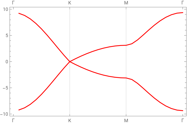
2,0; a2=a {1,0,0};A={0,0,0}; B=(a1+a2)/3;{guc,T,a0} = {{A,B},{a1,a2},a0};Define the line of interest in the reciprocal space of graphene and sample -points along this path (here we define the lines connecting high symmetry points , , of the first Brillouin zone of graphene):
k
Γ
K
M
Γ={0,0,0};K={4π/(3a),0,0};M=,-,0;np=10;klist=JoinTable(K-Γ)+Γ,{i,np},Table(M-K)+K,{i,np},Table(Γ-M)+M,{i,np};
π
a
π
3
ai
np
i
np
i
np
Calculate the eigenvalues of the Hamiltonian in each -point:
k
el=Sort@Chop@Eigenvalues[Hamiltonian[{guc,guc},TranslationVectors{{a1,a2},{a1,a2}},Kpoint#]]&;bands=el/@klist;
Transform the collected data by into the format suitable for and visualize the electronic energy bands along the chosen path:
ListLinePlot[Transpose[bands],PlotStyleRed,AxesFalse,FrameTrue,FrameTicks{{{0,"Γ"},{10,"K"},{20,"M"},{30,"Γ"}},Automatic},GridLines{{10,20},None}]
ElectronicStructure
ElectronicStructure
2D band structure
2D band structure
◼
Graphene
Take graphene lattice parameters
a0=1.42; a=
3
a0;a1=a 12,3
2,0; a2=a {1,0,0};A={0,0,0}; B=(a1+a2)/3;{guc,T,a0} = {{A,B},{a1,a2},a0};Sample a square patch in the reciprocal space that is large enough to cover the first Brillouin zone with -points along each of the edges:
50
k
np=50;klist=Flatten[Table[{kx,ky,0},{kx,-2,2,4/(np-1)},{ky,-2,2,4/(np-1)}],1];
Calculate electronic energy bands for the generated list of -points:
k
bands=ElectronicStructure[{guc,guc},TranslationVectors{{a1,a2},{a1,a2}},Kpointklist];
Transform conduction band data to the form acceptable by or :
cband=MapThread[{#1〚1〛,#1〚2〛,#2}&,{Last[bands],bands〚2〛}];
Visualize obtained conduction band with :
ListPlot3Dcband,AxesLabel", ",", ","E, eV",PlotStyleDirective[Opacity[0.7]],MeshNone,RegionFunctionFunction[{x,y,z},x^2+y^2<],ColorFunction"TemperatureMap",MeshFunctions->{#3&},ImageSize{330}
k
x
-1
Å
k
y
-1
Å
2
(1.8)

◼
Bilayer graphene
Set up bilayer graphene lattice parameters:
a0=1.42; a=
3
a0; c=3.35; a1=a 12,3
2,0; a2=a {1,0,0}; a3 = c {0,0, 2};A={0,0,0};B=(a1+a2)/3;{bguc,T,a0} = {{A,B,A+B+a3/2,2 B+a3/2},{a1,a2,a3},a0};Define nearest neighbor vectors for A and B sublattices:
nnB={A-B,A+a1-B,A+a2-B};nnA=-nnB;
Using this difference, we can define a couple of test functions (see full documentation of the TBpack application) that can be used for a subtle setting of the hopping integrals in the graphene bilayer accounting for hoppings between the sublattices with different atomic surroundings:
(* test for the alignment of two vectors *)codirQ=If[(#1-#2).(#1-#2)<,True,False]&;(* test for the crystal on-site potential *)test0=Or@@Flatten@Outer[codirQ,#7〚2,2〛,nnB,1]&&Round0||Or@@Flatten@Outer[codirQ,#7〚2,2〛,nnA,1]&&Round1&;(* test for the interlayer intersublattice hopping integral *)test3=(Or@@Flatten@Outer[codirQ,#7〚2,2〛,#8〚2,2〛,1])&;
-4
10
#7〚1,3〛
c
#7〚1,3〛
c
Band structure along the path
Band structure along the path
◼
Trilayer graphene
Take ABA-staked trilayer graphene lattice parameters:
Set up nearest neighbor vectors for A and B sublatices:
EdgeCorrections element lengths must be also adjusted to the new lengths of HoppingIntegrals, OverlappingIntegrals and HoppingDistances options.
Visualize the four subbands that are the closest to the intrinsic Fermi level in the system:
The resulting plot is the same as that in Fig. 8 (b) of B. Partoens and F. M. Peeters, Phys. Rev. B 74, 075404 (2006).
ElectronicBands1D
ElectronicBands1D
Energy bands
Energy bands
◼
Single wall carbon nanotube
Take the list of atomic coordinate for armchair carbon nanotube (5,5):
Calculate the electronic energy band structure with default options of ElectronicBands1D:
How to get full experience of TBpack application
How to get full experience of TBpack application
Now that you have put your hands on the TBpack functions, you may want to get a full experience of TBpack application with documentation built-in into the Mathematica Documentation Center, available off-line and supported by a range of visualization and data analysis functions. To install the application, simply evaluate the next cell: