Density of States in Nanoplatelets
Density of States in Nanoplatelets
V. Khachatryan, M. Mkrtchyan
Wolfram Labaratory, Russian-Armenian University, Yerevan, Armenia
In our laboratory we are engaged in numerical modeling of processes in nanostructures, using Wolfram Language. In particular, we study optical and light phenomena to quantum dots, such as: interband absorption, photoluminescence, intraband absorption, nonlinear absorption, harmonic generations in quantum dots and much more. In this paper, we will show how to compare numerical and analytical results.
Introduction
Introduction
The density of states (DOS) is a fundamental concept in quantum physics, playing a critical role in analyzing the properties of nanostructures such as quantum dots, wires, films, and other systems exhibiting strong quantum effects. Unlike bulk materials, where the energy spectrum is nearly continuous, nanostructures exhibit quantized energy levels due to spatial confinement, and the distribution of available states becomes discrete, highly dependent on geometry and environmental conditions.Studying and calculating the DOS allows us to understand which energy levels are accessible to particles, how electronic and thermal transport behaves, how optical responses change, and how structural parameters influence the system. This knowledge is crucial for designing functional components in nanoelectronics, quantum photonics, and sensor technologies.There are several methods for calculating the density of states, each with distinct features: 1) Analytical approaches apply to idealized models with simple geometry (e.g., infinite quantum wells) and provide exact expressions for the DOS. 2) Numerical methods, such as finite difference and finite element methods, enable simulations of systems with arbitrary potential profiles by solving the Schrödinger equation on a spatial grid. 3) Density functional theory (DFT) accounts for electron interactions and is used for real materials, incorporating atomic structure and electron-electron correlations. 4) Green’s function formalism and density matrix techniques are used to analyze open quantum systems, describing tunneling currents and nonequilibrium states. 5) Statistical methods, including Monte Carlo simulations, are applied to study disorder, fluctuations, and thermal effects.
Constants
Constants
Electron states in Nanoplatelets
Electron states in Nanoplatelets
Let us to consider the single-particle states of charge carriers in the CdSe Nanoplatelets [1-3]. The Hamiltonian of a problem is written as follows:
In[]:=

Out[]=

where is Laplace operator, ℏ is reduced Plank constant, (z),(x,y) are confiniment potentials in nanoplatelet, (z) potentail along z-direction connected with polarization effects (in such structures, the effects of polarization in the z-direction cannot be ignored due to the significant difference in the dielectric constant between the NPL and the surrounding materials).
Δ
ρ(z)
U
conf
U
conf
U
self
In this paper, the Takagahara model [4-6] is used as (z) model
U
self
Out[]=
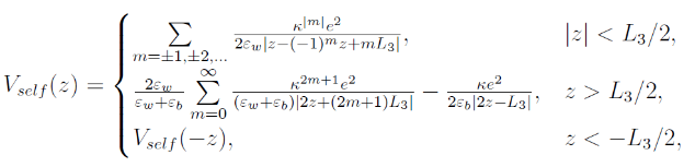
where and are NPL and its surrounding material dielectric constants, is a NPL length in axial direction. In WL code
ϵ
w
ϵ
b
L
3
In[]:=
ClearAll[Vself];Vself[ϵw_, ϵb_, n_] :=
The confining potential defined by the band offset between the NPL and its surrounding material is taken as a finite potential well:
Out[]=

Finally, the motion in direction is confined with confinement and self-potentials: z :
Out[]=

For the radial part we have:
Out[]=

These problems can be solved numerically by finite elements method:
In[]:=
ClearAll[Ez];Ez[ϵw_, ϵb_, n_, nz_]:=
In[]:=
ClearAll[Er];Er[ϵw_, ϵb_, n_, {lx_, ly_}, nr_]:=
where n is the monolayers number in NPL, and are NPL lenghts in x and y directions.
l
x
l
y
Density plot
Density plot
Now we can plot DOS in our NPL system. We know that DOS in nanophysics describes how many quantum states are available at each energy level for particles like electrons to occupy. To picture it simply — imagine an energy ladder. The density of states tells you how many “steps” are available at each energy height. The more available “steps” there are at a certain energy, the higher the probability that a particle (like an electron) will exist at that energy. In quantum nanostructures, the DOS isn’t smooth and continuous like in bulk materials—it becomes discrete or spiky due to spatial confinement. This means particles can only exist in specific allowed states, determined by the structure’s size and shape.
Out[]=


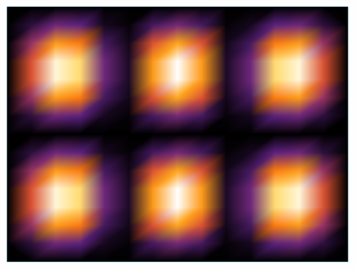
Based on the results, several main conclusions can be made:
1. The increase in the dielectric constant of both the environment and the NPL does not play a decisive role in the formation of the electronic properties of the NPL. If we compare them with each other, the dependence of the system on the permittivity of the environment is more pronounced.
2. As expected, an increase in the number of monolayers reduces the total energy of the system, due to a decrease in the effect of dimensional quantization in the system, while the localization of the electron cloud in one position also decreases.
3. Of course, the most significant factor in changing the behavior of the system is a change in the quantum state (in our case, the radial state and fixed axial), the energy of the system increases, and also, depending on the state, the important areas of localization of the electron cloud increase.
4. The dependences on the radial dimensions of the nanoplate are also considered, here again a decrease in size leads to a significant increase in the influence of the walls and, as a result, an increase in the energy of the system and a change in the possible localizations of the electron.
References
References
1. B. Mahler, B. Nadal, C. Bouet, G. Patriarche, B. Dubertret, Core/shell colloidal semiconductor nanoplatelets, Journal of the American Chemical Society 134 (45) (2012) 18591–18598.
2. D. A. Baghdasaryan, V. A. Harutyunyan, D. B. Hayrapetyan, E. M. Kazaryan, S. Baskoutas, H. A. Sarkisyan, Exciton States and Optical Absorption in CdSe and PbS Nanoplatelets, Nanomaterials 12 (2022).
3. B. T. Diroll, B. Guzelturk, H. Po, C. Dabard, N. Fu, L. Makke, E. Lhuillier, S. Ithurria, 2D II–VI semiconductor nanoplatelets: From material 12 synthesis to optoelectronic integration, Chemical Reviews 123 (7) (2023) 3543–3624
4. N. S. Rytova, Screened potential of a point charge in a thin film, Proc. MSU, Phys., Astron. 30 (3) (1967).
5. L. Keldysh, Coulomb interaction in thin semiconductor and semimetal films, in: Selected Papers of Leonid V Keldys, World Scientific, 2024, pp. 155–158.
6. M. Kumagai, T. Takagahara, Excitonic and nonlinear-optical properties of dielectric quantum-well structures, Physical Review B 40 (18) (1989) 12359.